Our Services
Wafer Level Packaging
Wafer Level Packaging (WLP) is among the most advanced packaging techniques in the semiconductor industry enabling chips to be packaged at wafer scale before dicing, resulting in smaller form factors, better electrical performance, and lower manufacturing cost per unit.
At India Chip, WLP is delivered using gold bumping interconnect technology, enabling high-density, high-reliability connections between the die and the substrate. Our WLP capability is optimised for Display Driver ICs components where miniaturisation and signal integrity are critical and is designed to meet the requirements of global display manufacturers serving mobile, consumer, and automotive markets.
What this means for customers: Smaller, faster, more reliable chips. Packages designed for the performance demands of modern display technology. Consistency and yield at production scale.
Chip Probing
Before a wafer is diced and its dies packaged, every single die must be electrically tested. Chip probing is this process a high-precision, automated testing operation that identifies which dies meet specification and which do not, ensuring that only known-good dies proceed to packaging.
At India Chip, chip probing is performed with the rigour that Display Driver IC applications demand. Our probing capability covers parametric testing, functional verification, and reliability screening, giving customers confidence in the integrity of every chip that leaves our facility. Effective probing directly improves packaging yield, reduces waste, and lowers the overall cost of production.
What this means for customers: Higher yield. Lower cost. Certainty that every packaged chip has been verified before value is added to it.
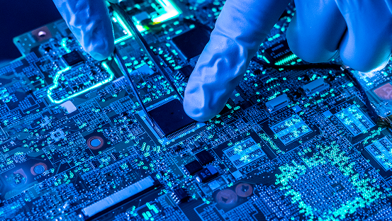
Die Processing
Once a wafer has been probed and diced, individual dies must be handled, prepared, and processed with extraordinary care. Die processing encompasses the precision steps between wafer singulation and final packaging including die attach, surface preparation, and quality inspection all performed in controlled environments to prevent contamination or damage to microscopic structures.
At India Chip, die processing is executed with the exacting standards that Display Driver IC technology requires. Our processes are designed to maintain the structural and electrical integrity of each die through every handling step, ensuring that the precision of the fab is preserved all the way to the finished package.
What this means for customers: Zero compromise between wafer and package. Process consistency. The reliability standards that automotive, consumer, and industrial display applications require.